Showing posts with label Digital Design. Show all posts

Thursday, October 10, 2019

Systemverilog simulators related

performance profile

VCS:
    profile in VCS by time or memory.
    #for memory profiling
        -simproile    //compile option
        -simprofile mem    //simulation option
    #for time profiling
        -simprofile    //compile options
        -simprofile time    //sim options
    the profile report will be store at compile directory named "profilereport"

IUS:
    debug sim hang by using cpu usage report
    compile option: -linedebug
    simulation option: -profile
    at sim hang point, stop test by: Ctrl+c (1 time), then ncsim>exit
    check the ncprof.out file (cpu usage summary and source code location)

Coverage

code coverage fefinition:
line/statement: will not cover module/end module/comments/time scale
block: begin...end, if...else, always
expression:
branch: case
conditional: if...else,  ternary operator (?:)
toggle:
FSM:

VCS:
%vcs -cm line+tgl+branch source.v
%simv -cm branch

vcs urg (Unified Report Generator):
%urg -dir simv1.vdb [simv2.dir simv3.vdb ...] -metric line+cond+branch -report specified_ouput_dir    //general options
%urg ... -parallel -sub bsub -lsf ""    //run urg in parallel to speed up
%urg -elfile <filename>    //for exclusion files
%dve -covdir simv.vdb//view coverage db directly in DVE

Dump Waveform

1. Options
setenv FSDB_FORCE    //to display forced signals in highlight in waveform viewer
2. sdf
3. use do file to control fsdb dump.
%vcs -ucli -do PATH_OF_DO_FILE    //simulation options
below is a sample tcl do file:
####start of file###############
#control fsdb dump
set run_time_before_dump 0us
set dump_all 1
set run_time 400us
run $run_time_before_dump
set TOP eth_top_tb
fsdbDumpfile $TOP.fsdb
if (dump_all == 1) {
    fsdbDumpvars 3 $TOP
    fsdbDumpvars 0 $TOP.xxx...
    fsdbDumpMDA 1 $TOP...
} esel {
    ...
}
run $run_time
exit
####end of file################
4.dump force information
simv +fsdb+force
5.dump glitch info
Before VCSMX/1509, 
simv +fsdb+sequential +fsdb+glitch=0 +fsdb+region
+fsdb+glitch=num,0表示所有的glitch都保存,1表示最近的glitch保存,2表示最近两个glitch被保存 
After VCSMX/1509, 
simv +fsdb+delta

Race Condition

VCS:
+evalorder    //vcs sim option
                     //eval combinational group then behavioral group.
                     //reduce race, refer to vcs userguide

Monday, September 30, 2019

Physical layer of Networking Hardware

prbs generator:

Random bit sequence using Verilog
prbs polynomials used in networking
Fibonacci form and Galois form

Fibonacci form: Another unique feature to this form is that the values in the shift register aren’t modified between when they are originally calculated and the output–making it possible to see then next LN output bits by just examining the shift register state. 

I have seen it used for prbs(peudo random binary sequence in ethernet transmission protocols for scrambler/descrambler, encoding pad, random pattern generation for loopback testing, Cyclic redundancy check(CRC) and so on), timer( non linear incremental timer, as lfsr normally has a fixed perioed)

References:
wiki
Generating Pseudo-Random Numbers on an FPGA
An example LFSR


ADC OSC(oversampling ratio):

The basics of sigma delta analog-to-digital converters
Delta-sigma modulation

Explaining SerDes:
(Chinese) SerDes Knowlege: notice the limitations of parallel transmission.

circuit noises:

simultaneously switching noise an overview/

Tuesday, August 27, 2019

Digital Design Verification Subsystem Lessons Learned


  1. make bus randomized during invalid cycle, to catch dut bugs that did not check valid signals. However, the constraint should still give 0 bus value a weight, so that 0 bus value can happen in invalid cycle, just in case that in real chip, the bus value is gated to 0 by upper layer module.
  2. bugs of features that cross two subsystems are difficult to catch. if a value generated in one module, and will be used in next module, it has a higher chance to have bug uncatched, as it needs correct model behavior as real hardware. solution: a) it's better to try to implement this in the same module, instead of split it into different modules, if possible. an example is the idle insertion/deletion to accommodate the AM (alignment marker) insertion/deletion in PCS. in this case, it's better to implement it in PCS instead of in MAC.
  3. bugs of features that related to performance AND cross two subsystems are extremely difficult to catch. possible solutions: a) in subsystem level, force to speed up counter value count, and increase pkt counts and so on, so that the possibility is increased. however, this needs very specific test scenarios; b) use hardware acceleration or e, e.g. Palladium or Synopsys ZeBu; c) chip top test to simulate the cross subsystem behaviors
  4. simplify architecture based on real application. sometimes, smart design means simple brutal force. this one needs the architects sensitivity to the industry use scenarios. I have two examples: a) initially we design our switch to have all kinds of protocols and features to both be legacy device compatible and also includes new features. this leads to overdesign and many bugs (insufficient man power and verification time). however, data center ethernet switch are more focused on feed and speed, it needs high throughput, less focused on protocols. end results, a lot of features are not used, a lot of hot new architectures (like SDN) are not used. this is big waste of resources. b) ...?
  5. Review every registers with DE in review meetings. Need to decide for every register: a) what is its meaning and actual use case (e.g. how does software guy config it, how does SA test it in real chip); b) can it be randomized in base test or should be tested in specific test; c) does it have some values that are often used by SA and Customer in real chip? weighted distribution?
  6. Review base config randomization constraints for base test. this is also related to 5) as some of the configs are registers. it needs designer and SA's input to confirm.
  7. simulation time vs packets number: Do Not trade packets number for simulation time. Meaning that do not try to save hardware resources. For verification, the first priority is function correctness, and the more packet number, the more possible that a bug will be hit. CPU resources are cheap, real chip bugs are expensive!
  8. random noise register/memory access during every test. But make sure that the noise and actually traffic can actually hit the same register/memory to trigger corner bugs.
  9. there should be 2 types of checker for a features if it cannot be accurately checked in every scenarios: a) a specific test that accurately check it's function; b) a general checker which is enabled in every testcase, and act as a sanity checker, in case there is some fundamental bugs in certain corner cases, which was not found in the a).
  10. choose the constraint range carefully, and choose the random value carefully. speed mode, pkt number, and the event happen time are all related, need to consider them when setting constraint or randomization range.
  11. have status and counters for monitors and controlling tb in cfg or virtual interface. for example, have counter count received pkt count, or have status variable to monitor dut is in transmiting or idle state, and so on.

Tuesday, August 20, 2019

Protocols

1. IIC or I²C (Inter-Integrated Circuit)

– Bus topology / routing / resources:

From this point of view, I²C is a clear winner over SPI in sparing pins, board routing and how easy it is to build an I²C network.

– Throughput / Speed:

If data must be transferred at ‘high speed’, SPI is clearly the protocol of choice, over I²C. SPI is full-duplex; I²C is not. SPI does not define any speed limit; implementations often go over 10 Mbps. I²C is limited to 1Mbps in Fast Mode+ and to 3.4 Mbps in High Speed Mode – this last one requiring specific I/O buffers, not always easily available.

– Elegance:

Both SPI and I2C offer good support for communication with low-speed devices, but SPI is better suited to applications in which devices transfer data streams, while I²C is better at multi master ‘register access’ application.

Conclusions.

In the world of communication protocols, I²C and SPI are often considered as ‘little’ communication protocols compared to Ethernet, USB, SATA, PCI-Express and others, that present throughput in the x100 megabit per second range if not gigabit per second. Though, one must not forget what each protocol is meant for. Ethernet, USB, SATA are meant for ‘outside the box communications’ and data exchanges between whole systems. When there is a need to implement a communication between integrated circuit such as a microcontroller and a set of relatively slow peripheral, there is no point at using any excessively complex protocols. There, I²C and SPI perfectly fit the bill and have become so popular that it is very likely that any embedded system engineer will use them during his/her career.

2. RTC (Real-Time Clock)
3. UART(Universal Asynchronous Receiver/Transmitter)
freebsd Serial and UART Tutorial
    The Start bit always has a value of 0 (a Space). The Stop Bit always has a value of 1 (a Mark). This means that there will always be a Mark (1) to Space (0) transition on the line at the start of every word, even when multiple word are transmitted back to back. This guarantees that sender and receiver can resynchronize their clocks regardless of the content of the data bits that are being transmitted. refer to stm32f103 reference manual S.27.3.3: 16X oversampling was used to detect noise errors.

4. ARM AMBA

Read Transaction:
To start the transaction off, the master places the slave's address on the ARADDR line and asserts that there is a valid address (ARVALID). Following time T1, the slave asserts the ready signal (ARREADY). Remember the source of data asserts the valid signal when information is available, while the receiver asserts the ready signal when it is able to consume that information. For a transfer to occur both READY and VALID must be asserted. All of this happens on the read address channel, with the address transfer completing on the rising edge of time T2.


From here, the rest of the transaction occurs on the read data channel. When the master is ready for data it asserts its RREADY signal. The slave then places data on the RDATA line and asserts that there is valid data (RVALID). In this case, the slave is the source and the master is the receiver. Recall that VALID and READY can be asserted in any order so long as VALID does not depend on READY. This read represents a single burst transaction made up of 4 beats or data transfers. Notice the slave asserts RLAST when the final beat is transferred.

Write Transaction:
What about writes? Figure 3 shows a timing diagram of an AXI write transaction. The addressing phase is similar to a read. A master places an address on the AWADDR line and asserts a valid signal. The slave asserts that it's ready to receive the address and the address is transferred. 
Next, on the Write Data Channel, the master places data on the bus and asserts the valid signal (WVALID). When the slave is ready, it asserts WREADY and data transfer begins. This transfer is again 4 beats for a single burst. The master asserts the WLAST when the last beat of data has been transferred. 
In contrast to reads, writes include a Write Response Channel where the slave can assert that the write transaction has completed successfully.


AXI Interconnect:
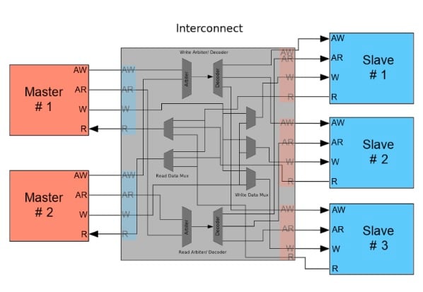
This is where AXI provides the most flexibility. Instead of prescribing how multi-master and multi-slave systems work, the AXI standard only defines the interfaces and leaves the rest up to the designer. If the system has multiple masters attempting to communicate with a single slave, then the AXI Interconnect may contain an arbiter that routes data between the master and slave interfaces. This arbiter could be implemented using simple priorities, a round-robin architecture, or whatever suits the designer's needs.

Systems that use multiple masters and multiple slaves could have interconnects containing arbiters, decoders, multiplexers, and whatever else is needed to successfully process transactions. This might include logic to translate between AXI3, AXI4, and AXI4-Lite protocols. 
Additionally, interconnects can perform bus-width conversion, use data FIFOs, contain register slices to break timing paths, and even convert between two different clock domains.

Burst len, size, type:

The burst length for AXI3 is 1~16, for AXI4 is 1~256(INCR) and 1~16(other burst type)

Burstsize: the maximum number of bytes to transfer in each data transfer, or beat, in a burst. 
If the AXI bus is wider than the burst size, the AXI interface must determine from the transfer address which byte of lanes of the data bus to use for each transfer. See Data read and write structure on axi spec. 

The size of any transfer must not exceed the data bus width of either agent in the transaction. 


Out of order: 

Data from read transaction ARID values can arrive in any order

Interleave:

Read data of transaction with different ARID values can be interleaved
Write Interleaved: AXI3 support, but the first item of write data must be issued in the same order as the write address. AXI4 does not support interleave. 

Unaligned Address:

TODO

AXI response


5. USB2.0
USB2 made simple(better and low level)
USB in a nutshell(introductory)

6. SPI

Wednesday, July 10, 2019

Ethernet Protocol Notes

Gigabit Ethernet:
this post is about 1G Physical Coding Sublayer (PCS), and explains scrambler/descrambler. Note the way it explains Bit Error Rate (BER).
Gigabit Ethernet 1000BASE-T

scrambling -> Spread Spectrum

Thursday, May 30, 2019

Digital Design and Computer Architecuture Study Notes

Bottome-up progression:

Number system -> Boolean algebra -> Boolean algebra using electrical switches -> Logic Gates -> addition (base of all calculation) -> subtraction -> combinational(NO FEEDBACK) without feedback, value change immediately (unstable) & sequential(FEEDBACK) feedback can make state(stable) -> memory, calculation without memory is not very useful -> Conditional Jump (Controlled repetition or looping is what separates computers from calculators.)

Power Consumption:

-Pdynamic = 1/2*CVDD**2f; Voltage on the capacitor switches at frequency f, it charges the capacitor f/2 times and discharges it f/2 times per second. Discharging does not draw energy from the power supply.

-Pstatic = IDD*VDD

Logic Gates:

-NOT Gate, Buffer, AND Gate, OR Gate, XOR, NAND, NOR, Transmission Gate

Combinational Logic:

characterized by its propagation delay and contamination delay. The propagation delay, tpd, is the maximum time from when an input changes until the output or outputs reach their final value. The contamination delay, tcd, is the minimum time from when an input changes until any output starts to changes its value.
Combinational logic has no cyclic paths and no races. If inputs are applied to combinational logic, the outputs will always settle to the correct value within a propagation delay.

-Building blocks: full adders, seven-segment display decoders, multiplexer, decoder, priority circuits, arithmetic circuits

-Boolean algebra

-Karnaugh maps: works well for problems with up to four variables. More importantly they give insight into manipulating Boolean equations. Gray code. Dont care for output can be treateed as either 0's or 1's at the designer's discretion.

-Glitches: insight from Karnaugh maps

Sequential Logic:

SR Latch:
D Latch: copies D to Q when clk is 1
D flip-flop: copies D to Q on the rising edge of the clock, and remembers it's state at all other times

synchronous sequential circuit composition teaches us that a circuit is a synchronous sequential circuit if it consists of interconnected circuit elements such that:
-Every circuit element is either a register or a combinational circuit
-At least one circuit element is a register
-All registers receive the same clock signal
-Every cyclic path contains at least one register

-Building blocks: arithmetic circuits, counters, shift registers, memory arrays, and logic arrays.

Finite state machine:

-An FSM consists of two blocks of combinational logic, next state logic and output logic, and a register that stores the state.
-There are two general classes of finite state machines: Moore machines (the outputs depend only on the current state of the machine), and Mealy machines (the outputs depend only on both the current state and the current inputs).
-HDL descriptions of state machines are correspondingly divided into three parts to model the state register, the next state logic, and the output logic.

Verilog Blocking and Nonblocking Assignement:

-Use always @ (posedge clk) and nonblocking assignments to model synchronous sequential logic.
    always @ (posedge clk)
      begin
        n1 <= d; //nonblocking
        q <= n1; //nonblocking
      end

-Use continous assignments to model simple combinational logic.
    assign y = s ? d1 : d0;

-Use always @ (*) and blocking assignments to model more complicated combinational logic where the always statement is helpful
(A case statement implies combinational logic if all possible input combinations are defined; otherwise it implies sequential logic, because the output will keep its old value in the undefined cases.)
(If statement implies combinational logic, if all possible inputs combinations are handled; otherwise it produces sequential logic.)
(It is good practice to use blocking assignments for combinational logic and nonblocking assignments for sequential logic.)
(Signals in always statement and initial statement must be declared as reg type)
(Not that signal must be declared as reg because it appears on the left hand side of a <= or = sign in an always statement. Nevertheless, it does not mean it's the output of a register, and it can be the output of a combinational logic.)
    always @ (*)
        begin
            p = a^ b; //blocking
            g = a & b;//blocking
            s = p ^ cin;
            cout = g | (p & cin);
        end

-Do not make assignments to the same signal in more than one always statement or continuous assignment
-assign statemns must be used outside always statements and are also evaluated concurrently. a type of continuous assignment.
-case statement and if statements must appear inside always statements.

Verilog

-verilog provide generate statements to produce a variable amount of hardware depending on the value of a parameter. generate supports for loops and if statements to determine how many of what types of hardware to produce.

-The initial statement executes the statements in its body at the start of simulation. initial statements should be used only in testbenches for simulation, not in modules intended to be synthesized into actual hardware. Hardware has no way of magically executing a sequence of special steps when it is first turned on. Like signals in always statements, signals in initial statements must be declared to be reg.

-Testbenches use the === and !=== operators for comparisons of equality and inequality respectively, because these operators work correctly with operands that could be x or z.

-the For loop, can be either synthesizable, where it is used to simply expand replicated logic, and they do not loop like in a c program; it can also be non synthesizable, behave like a c program, can have delay in side, not in always statement?.


-Understand the following:
1) reg and wire (Berkeley CS150)
reg is a confusing term, it is used for anything that holds data. wire cannot retain any data, henceforth it must be driven by continuous assignments. 
read 2) to understand what is state.  

       wire: continuous assignment only, can resolve multiple driver. 

       reg: a language failure, it's just a varialbe, nothing to do with register. can hold varaible, therefore procedural assignment. cannot be multiple driver. can model both combinational and sequential logic.

2) Inferred Latch (stackoverflow)
3) blocking and non-blocking
4) a neat blinky
5) port connection data types wire or reg: (refer to Verilog HDL by Samire Palnitkar)
        port as internal unit and external input.
        any side that is the data source, it can be either types. (external inputs, or internal outputs)
        any side that is the data monitor, it must be net type so can be continuously assigned. (internal inputs, inout, or external outputs). a module instantiation is to connect the input/output signals continuously. so the internal input must be net, and the external output must be net, as it is implicitly driven continuously.

raspberry pi gpio controls

#gpiozero library https://gpiozero.readthedocs.io/en/stable/#